From Gerber to PCB in Altium: Master Your Professional PCB Design Workflow Via size calculators: sizing vias in your next multilayer pcbs
If you are searching about Raspberry Pi Printed Circuit Board (PCB) Diagram: Build Your Own IoT you've came to the right page. We have 12 Images about Raspberry Pi Printed Circuit Board (PCB) Diagram: Build Your Own IoT like Your Guide to Gerber File Extensions in PCB Design | Blog | Altium Designer, PCB Design for Manufacturing: Prevent PCB Vias Defects by Talking to and also Via Size Calculators: Sizing Vias in Your Next Multilayer PCBs | PCB. Read more:
Raspberry Pi Printed Circuit Board (PCB) Diagram: Build Your Own IoT
 diywiringtips.blogspot.com
Raspberry Pi Printed Circuit Board (PCB) Diagram: Build Your Own IoT ...
Access To Your Training Certificates On My Altium | Altium
 resources.altium.com
Access to your Training Certificates on My Altium | Altium
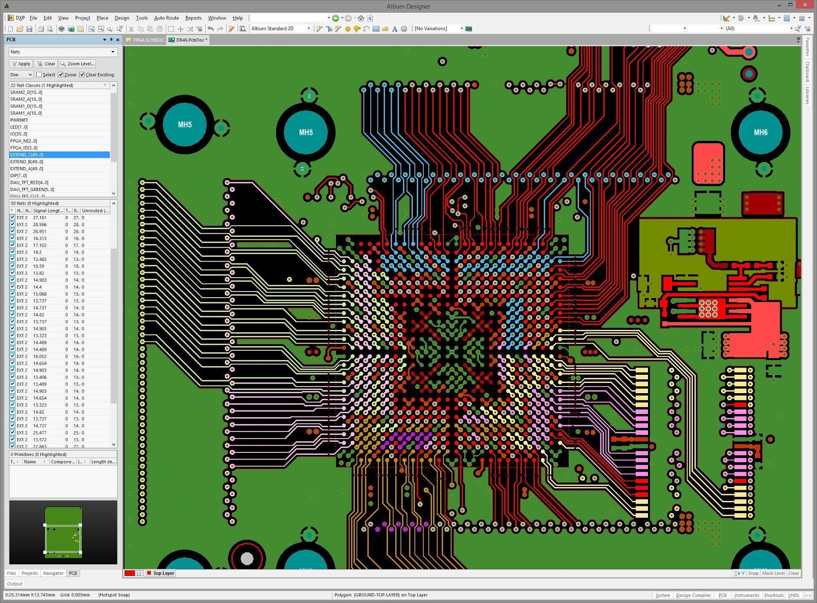
PCB Impedance Calculator And Stackup Design In Altium Designer
 resources.altium.com
PCB Impedance Calculator and Stackup Design in Altium Designer
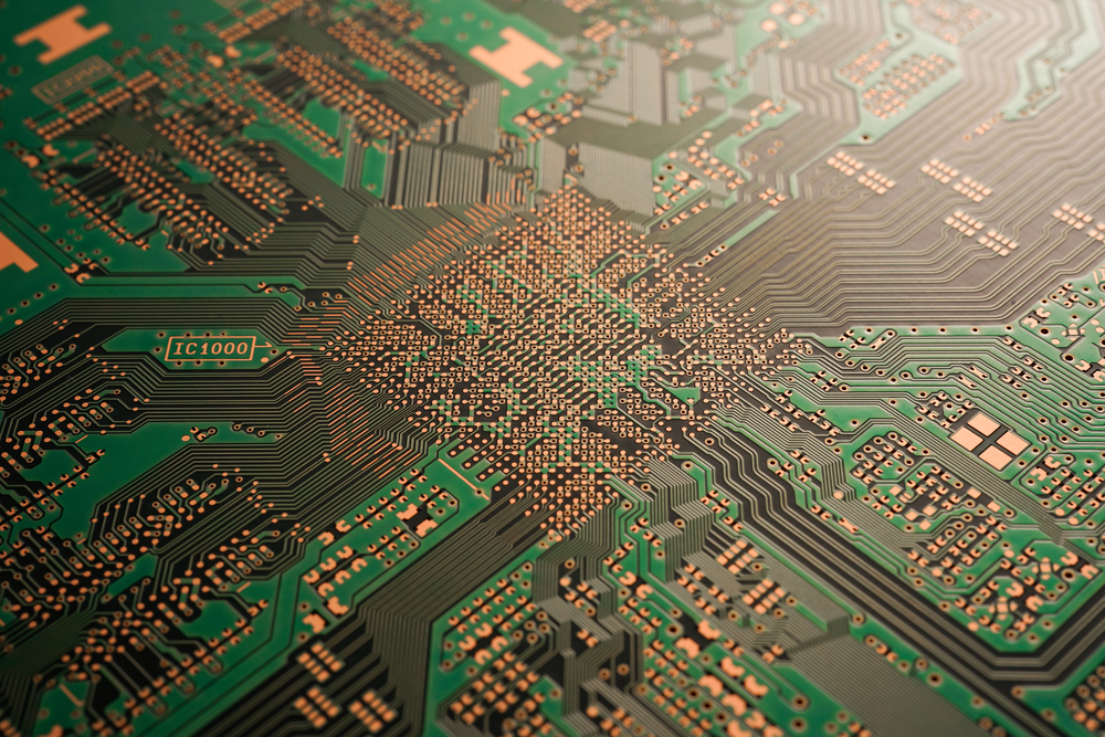
Altium Gerber Output: A Comprehensive Guide – Hillman Curtis: Printed
 hillmancurtis.com
Altium Gerber Output: A Comprehensive Guide – Hillman Curtis: Printed ...
Cómo Obtener Una Mejor Perspectiva De Su PCB Con Visualización A Color
 resources.altium.com
Cómo obtener una mejor perspectiva de su PCB con visualización a color ...
PCB Design For Manufacturing: Prevent PCB Vias Defects By Talking To
 resources.altium.com
PCB Design for Manufacturing: Prevent PCB Vias Defects by Talking to ...
Your Guide To Gerber File Extensions In PCB Design | Blog | Altium Designer
 resources.altium.com
Your Guide to Gerber File Extensions in PCB Design | Blog | Altium Designer
Via Size Calculators: Sizing Vias In Your Next Multilayer PCBs | PCB
 resources.altium.com
Via Size Calculators: Sizing Vias in Your Next Multilayer PCBs | PCB ...
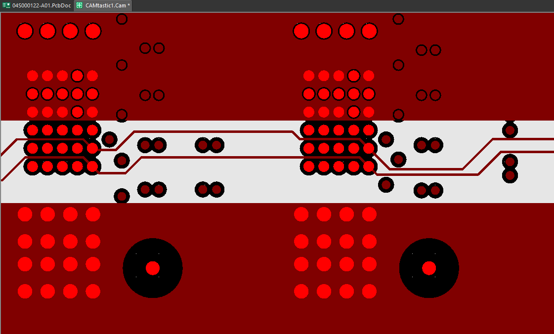
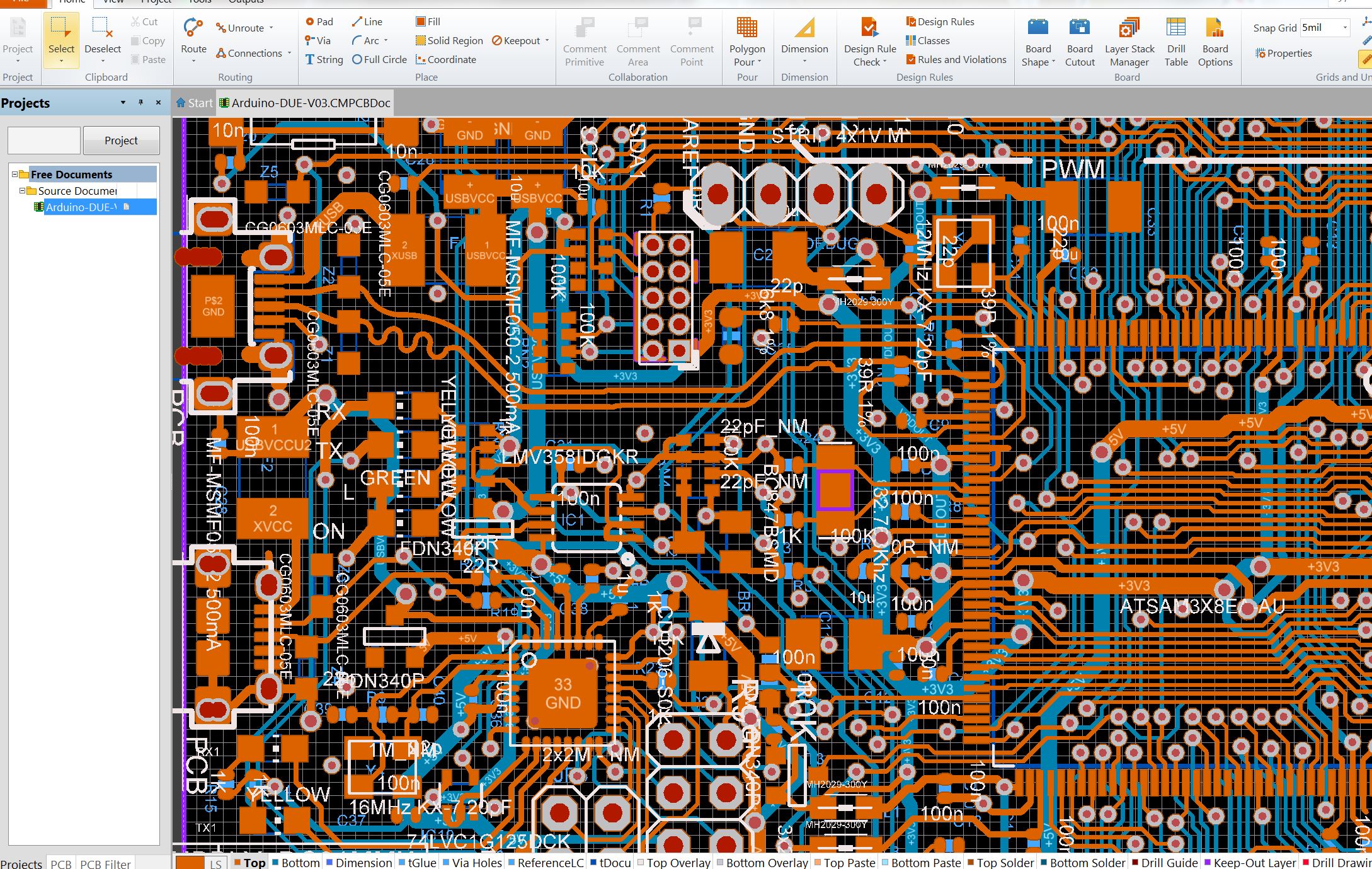
Editing PCBs With Gerber Files In Altium: A Comprehensive Workflow
 www.raypcb.com
Editing PCBs with Gerber Files in Altium: A Comprehensive Workflow ...
OrCAD Electronic Design And PCB Layout | FlowCAD
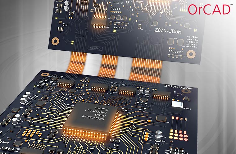 www.flowcad.com
OrCAD Electronic Design and PCB Layout | FlowCAD
Basic Steps To Design A PCB Layout | Quadcept Blog
 blog.quadcept.com
Basic Steps to Design a PCB Layout | Quadcept Blog
Altium CircuitMaker – PaxSpace, Inc
 www.paxspace.org
Altium CircuitMaker – PaxSpace, Inc
pcb impedance calculator and stackup design in altium designer. Altium gerber output: a comprehensive guide – hillman curtis: printed. Cómo obtener una mejor perspectiva de su pcb con visualización a color ...